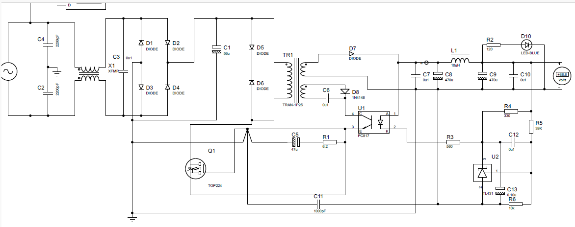
SWITCH MODE POWER SUPPLY
This Switch mode Power Supply uses a TOP224Y integrated circuit as the primary switching element. The TOP224Y is a flyback controller IC that is designed for high-efficiency switching power supplies. It has a built-in MOSFET and feedback loop to regulate the output voltage.
The circuit of switch mode power supply
The circuit works by first converting the incoming AC voltage to a DC voltage using the bridge rectifier (BR1). The DC voltage is then filtered by the capacitor (C1). The filtered DC voltage is then fed to the TOP224Y IC, which switches it at a high frequency to generate a high-voltage AC signal. The high-voltage AC signal is then transformed to a low-voltage AC signal by the transformer (TR1). The low-voltage AC signal is then rectified by the diode (D7) and filtered by the capacitor (C8) to produce the desired output voltage.
DESIGN CALCULATIONS
In a switching power supply circuit, inductor X1 plays a crucial role in smoothing out the pulsating DC voltage from the bridge rectifier and storing energy during the on-state of the switching transistor. The inductance value of X1 is determined by several factors, including the input voltage, output current, switching frequency, and desired ripple voltage.
Calculating Inductance Value:
The inductance value of X1 can be calculated using the following equation:
X1 = (V_in * T_on) / (I_ripple * ΔI)
where:
• V_in: Input voltage
• T_on: On-time of the switching transistor
• I_ripple: Desired ripple current
• ΔI: Peak-to-peak current change in the inductor
Bridge Rectifier Design
The bridge rectifier converts the incoming AC voltage to a pulsating DC voltage. The following parameters need to be considered when designing the bridge rectifier:
• Peak input voltage (V_peak): The peak input voltage is the maximum value of the AC voltage. It is typically 170 V for 120 V mains voltage.
• Average input current (I_avg): The average input current is the average current drawn by the circuit. It is determined by the following equation:
I_avg = P_output / V_dc
where P_output is the output power of the power supply and V_dc is the average DC voltage.
• Peak forward current (I_FM): The peak forward current is the maximum current that each diode in the bridge rectifier must handle. It is determined by the following equation:
I_FM = I_avg / 2
• Average reverse current (I_RM): The average reverse current is the average current that each diode in the bridge rectifier must block. It is typically very small.
• Forward voltage drop (V_F): The forward voltage drop is the voltage drop across each diode when it is conducting. It is typically about 0.7 V for silicon diodes.
Using the above parameters, we can select the appropriate diodes for the bridge rectifier. The diodes must have a peak forward current rating that is greater than or equal to I_FM, an average reverse current rating that is greater than or equal to I_RM, and a forward voltage drop that is less than or equal to V_F.
Input Capacitor Design
The input capacitor filters the pulsating DC voltage from the bridge rectifier. The following parameters need to be considered when designing the input capacitor:
• Input voltage ripple (V_ripple): The input voltage ripple is the amount of ripple in the pulsating DC voltage. It is typically specified as a percentage of the average DC voltage.
• Input capacitor capacitance (C_in): The input capacitor capacitance is determined by the following equation:
C_in = 4 * f_s * L * I_avg / V_ripple
where f_s is the switching frequency, L is the inductance of the primary winding of the transformer, and I_avg is the average input current.
• Input capacitor voltage rating (V_DC): The input capacitor voltage rating must be greater than or equal to the peak input voltage.
Using the above parameters, we can select the appropriate capacitor for the input filter. The capacitor must have a capacitance that is greater than or equal to C_in and a voltage rating that is greater than or equal to V_DC.
This section of the circuit is responsible for converting the DC voltage from the bridge rectifier to a high-frequency AC signal. The high-frequency AC signal is then transformed by the transformer to a lower AC voltage, which is then rectified and filtered to provide the desired output voltage.
Switching Transistor (Q1):
The switching transistor must be able to handle the switching voltage and current. The switching voltage is the peak value of the DC voltage from the bridge rectifier, which is about 330 V. The switching current is the peak value of the current through the inductor, which is determined by the following equation:
I_peak = V_in / (2 * L * f_s)
where:
• V_in is the input voltage
• L is the inductance of the inductor
• f_s is the switching frequency
Flyback Diode (D7):
The flyback diode must be able to handle the peak reverse current of the inductor. The peak reverse current is determined by the following equation:
I_FRM = V_in * T_on / (2 * L)
where:
• T_on is the on-time of the switching transistor
Inductor (L1):
The inductance of the inductor is determined by the input voltage, output current, switching frequency, and desired ripple voltage. The following equation can be used to estimate the inductance value:
L1 ≈ (V_in * T_on) / (ΔI * f_s)
where:
• ΔI is the desired ripple current
Capacitor (C1):
The capacitance of the capacitor is determined by the output voltage and the desired ripple voltage. The following equation can be used to estimate the capacitance value:
C1 ≈ (2 * T_on) / (R_load * V_ripple)
where:
• R_load is the load resistance
Inductor L1:
Inductor L1 serves as a high-frequency filter, smoothing out the AC voltage from the transformer and reducing ripple voltage before it reaches the rectification stage. The inductance value of L1 affects the ripple voltage and the efficiency of the circuit. A higher inductance value generally results in lower ripple voltage but also increases the size and cost of the inductor.
Design Calculation:
The inductance value of L2 can be estimated using the following equation:
L1 ≈ (V_out * T_on) / (ΔI * f_s)
where:
• V_out is the desired output voltage
• T_on is the on-time of the switching transistor
• ΔI is the desired ripple current
• f_s is the switching frequency
Assuming a desired ripple current of 100 mV, a switching frequency of 100 kHz, and an output voltage of 12 V, the inductance value of L1 can be estimated as:
L1 ≈ (12 V * 5 µs) / (100 mA * 100 kHz) ≈ 6 µH
In practice, a slightly higher inductance value may be chosen to provide a margin of safety and reduce ripple voltage further.Thats why we used 10uH.
Output Capacitor C8:
Output capacitor C8 acts as a low-pass filter, smoothing out any remaining ripple voltage from the rectified AC voltage and providing a stable DC output voltage. The capacitance value of C8 affects the ripple voltage and the transient response of the circuit. A higher capacitance value generally results in lower ripple voltage but also increases the size and cost of the capacitor.
Design Calculation:
The capacitance value of C8 can be estimated using the following equation:
C8 ≈ (2 * T_off) / (R_load * V_ripple)
where:
• T_off is the off-time of the switching transistor
• R_load is the load resistance
• V_ripple is the desired ripple voltage
Assuming a desired ripple voltage of 1000 mV, a load resistance of 2 Ω, and an off-time of 4.5 µs (assuming a 50% duty cycle), the capacitance value of C8 can be estimated as:
C8 ≈ (2 * 4.5 µs) / (2 Ω * 1000 mV) ≈ 450 µF
In practice, a slightly higher capacitance value may be chosen to provide a margin of safety and reduce ripple voltage further.
Output Diode D2:
Output diode D2 protects the circuit from reverse current flow when the load is disconnected or experiences a sudden change in voltage. This prevents damage to the components and ensures the proper operation of the circuit.


